
")
")
Z80 Single Board Computer SBC - CPU Board


- Details
- Category: Microprocessori
- Published on Wednesday, 12 December 2012 21:35
- Written by Luigi
- Hits: 3736
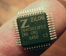
Z80 Single Board Computer
Z80 Embedded System
Z80 Embedded System
This story This article explains how to build a computer for embedded applications using a historical microprocessor that is still used in industrial automation, the Zilog Z80.
The first prototype is build around a PCB for each stage of the system; after all test, a second prototype with all the stages was made on only one PCB.
Let's start the adventure trying to understand the composition of the single stages:
The first prototype is build around a PCB for each stage of the system; after all test, a second prototype with all the stages was made on only one PCB.
Let's start the adventure trying to understand the composition of the single stages:
.: CIRCUIT :.
Due complexity of the circuit, to understand how this project works, you must first know the operation of the Z80 microprocessor. I will try to summarize the following in order to understand the various features.
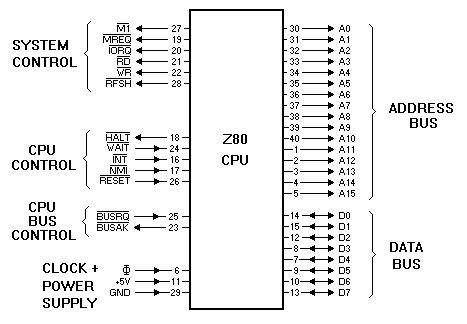
.: Z80 - PINOUT & CONNECTION :.
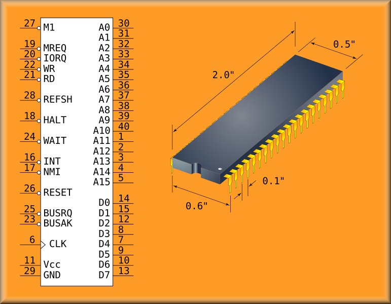
- pins A0 - A15 correspond to the connections of the ADDRESS BUS by which the microprocessor sets the address of a memory location or a device;
- pins D0 - D7 correspond to DATA BUS by which the microprocessor transfers data from its registers to memory and / or peripherals and vice versa;
- pins MREQ, IORQ, WR e RD correspond to the control signals of MEMORY and DEVICES;
- pins RESET, CLK, VCC, GND correspond to POWER SUPPLY and the basic signals for the operation of the MICRO;
- pins INT e NMI correspond to external INTERRUPT signals;
- pins BUSRQ e WAIT correspond to input signals that are usually not used;
- the rest of the PINS are not normally used. For the full explanation, refer you to the Z80 datasheet.
In order to work, therefore, the microprocessor, in addition to the power supply, needs two "satellite" units that generate the CLOCK signal and the RESET signal respectively.
The INT, NMI, WAIT and BUSRQ pins will be connected to logic level 1 (VCC) via a 10Kohm PULL-UP resistor.
The INT, NMI, WAIT and BUSRQ pins will be connected to logic level 1 (VCC) via a 10Kohm PULL-UP resistor.
.: Z80 - CLOCK CIRCUIT:.
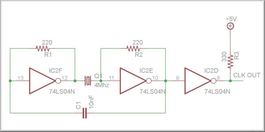
This is a simple clock generator made with the logic gates classic oscillator configuration.
.: Z80 - RESET CIRCUIT:.
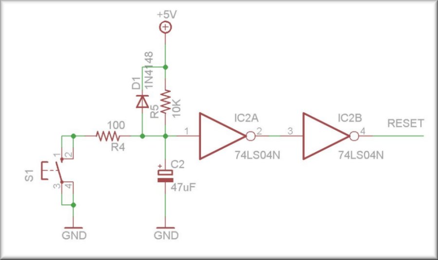
This is instead the RESET circuit.
It has a POR (Power On Reset) and a manual reset by pushing the button.
It has a POR (Power On Reset) and a manual reset by pushing the button.
.: Z80 - CPU-BOARD FULL CIRCUIT :.
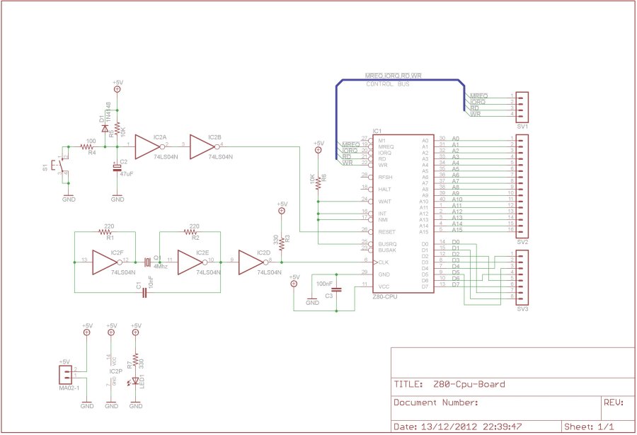
As can be seen from the diagram, pins INT, NMI, WAIT and BUSRQ are connected to the logic level 1 (VCC) by the R6 resistor.
The pin 26 has been applied to the RESET signal from the POR circuit and the CLOCK signal, from the CLOCK generator, was applied to pin 6.
C3 acts as decoupling on the power supply.
SV1, SV2 and SV3 allow the MICROPROCESSOR to communicate with the outside world (MEMORY and PERIPHERAL ).
The pin 26 has been applied to the RESET signal from the POR circuit and the CLOCK signal, from the CLOCK generator, was applied to pin 6.
C3 acts as decoupling on the power supply.
SV1, SV2 and SV3 allow the MICROPROCESSOR to communicate with the outside world (MEMORY and PERIPHERAL ).
.: Z80 - CPU-BOARD PCB :.
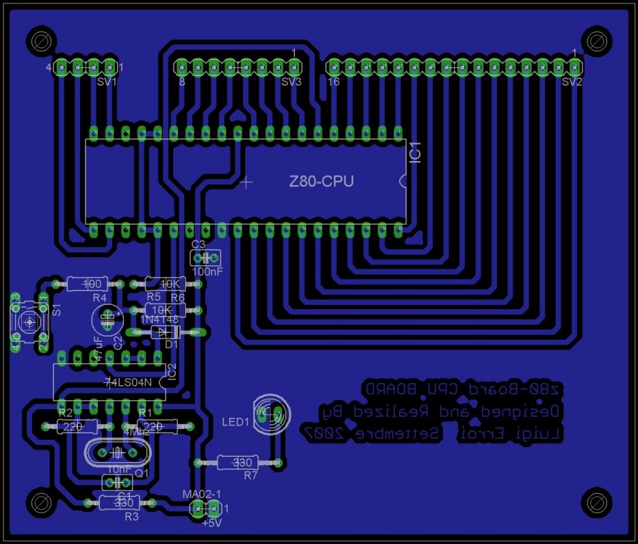
The above image shows the layout of the components on the printed circuit board of the CPU-BOARD board.
The board has also provided a signaling LED for the presence of the power supply.
The board has also provided a signaling LED for the presence of the power supply.
.: Z80 - CPU-BOARD :.
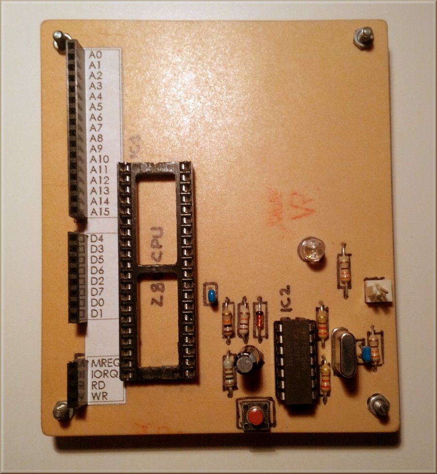
This is the realization of the board.
Alongside the output BUS, names of all lines have been reported to identify them quickly without the help of the component layout.
Alongside the output BUS, names of all lines have been reported to identify them quickly without the help of the component layout.

Caution!!! The right side for displaying the master in making the printed circuit is what reads the text.
As reported, the set is seen on the component side.
You will have to do a mirror of the print.
The file is in PDF format in order to avoid the proportional errors.
However, before printing I suggest that you test the 1: 1 print scale and not select "fit to the page ".
As reported, the set is seen on the component side.
You will have to do a mirror of the print.
The file is in PDF format in order to avoid the proportional errors.
However, before printing I suggest that you test the 1: 1 print scale and not select "fit to the page ".
| SCHEMTATIC | PCB | SERIGRAPHY |