
")
")
Z80 Single Board Computer SBC - BUS Board


- Details
- Category: Microprocessori
- Published on Wednesday, 12 December 2012 21:35
- Written by Luigi
- Hits: 2815
Z80 Single Board Computer
Z80 Embedded System
BUS Board - 2nd section
Z80 Embedded System
BUS Board - 2nd section
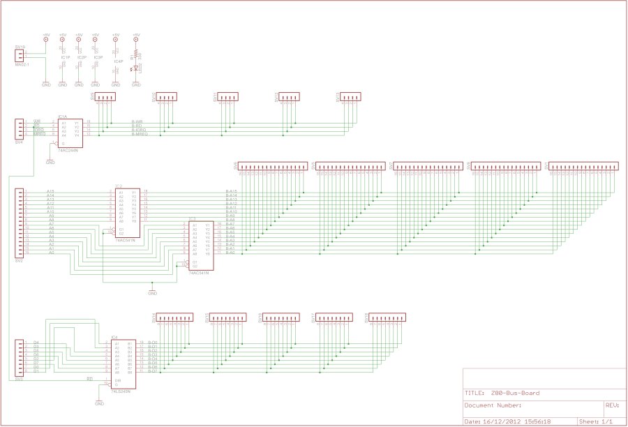
In this second section, we will describe a board that will interface the CPU-BOARD card with other devices, the BUS-BOARD card. Its purpose is to isolate the CPU from other peripherals connected to it and not overload its outputs. This is the BUFFER used to supply the correct amount of current needed for the various peripherals connected to the CPU BOARD.
The card is made with integrated circuits of the 74LS244, 74LS245 and 74LS541 series, which are basically line buffers.
The card is made with integrated circuits of the 74LS244, 74LS245 and 74LS541 series, which are basically line buffers.
.: CIRCUIT :.
The schematic consists of 3 integrated: 74LS244, 74LS245 and 74LS541.
1/2 74LS244 is used as a buffer for BUS control signals;
2x 74LS541 is used as buffer on BUS ADDRESSES; < and the 74LS245, bidirectional buffer, is used on the DATA BUS.
1/2 74LS244 is used as a buffer for BUS control signals;
2x 74LS541 is used as buffer on BUS ADDRESSES; < and the 74LS245, bidirectional buffer, is used on the DATA BUS.
.: Z80 - BUS-BOARD FULL CIRCUIT :.
.: Z80 - BUS-BOARD PCB :.

The above image shows the layout of the components on the printed circuit board of the BUS-BOARD board.
On the board, as in the previous one, a signal LED of the presence of power has been provided.
On the board, as in the previous one, a signal LED of the presence of power has been provided.
.: Z80 - BUS-BOARD :.
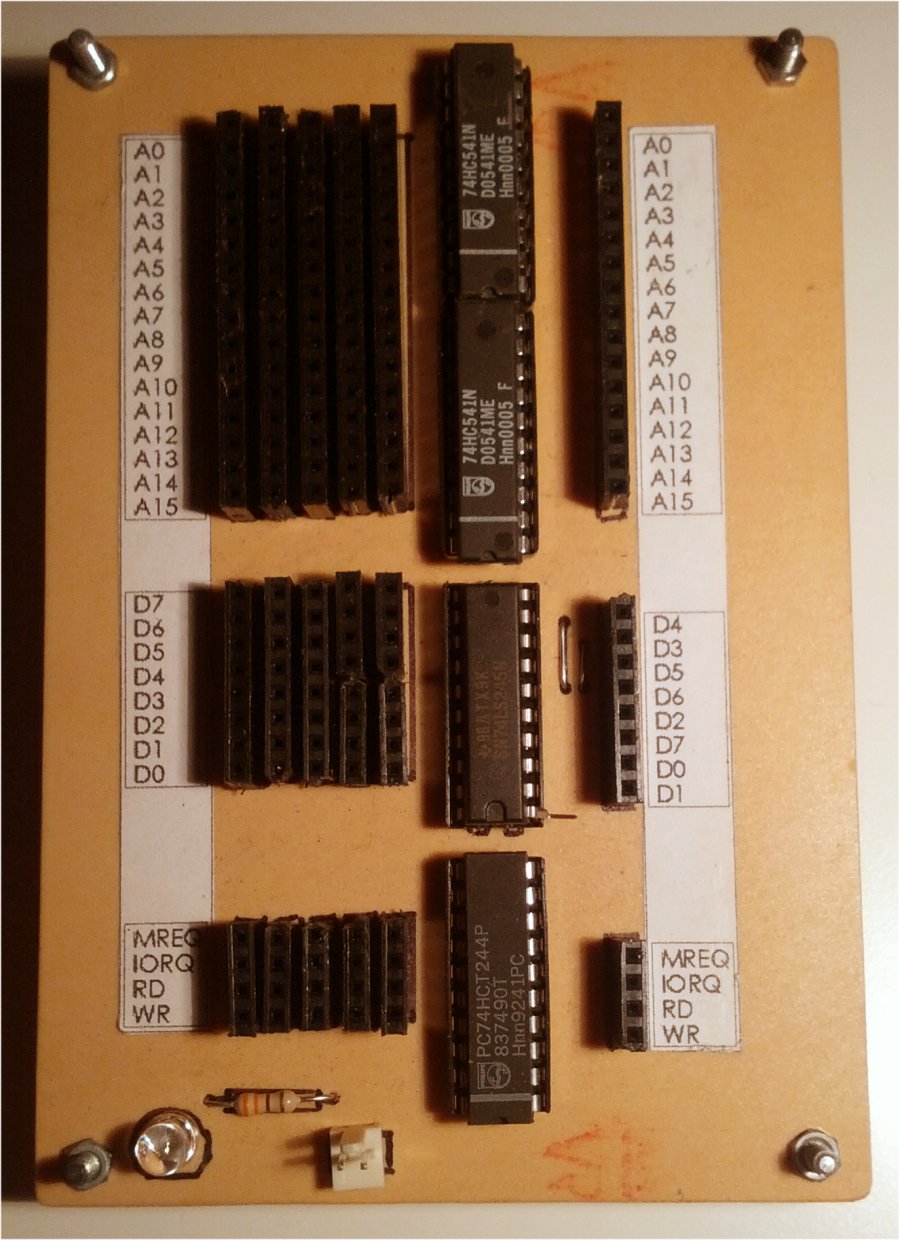
This is the realization of the board.
Alongside the output BUSs, as in the previous one, the names of all lines were reported to identify them quickly without the help of the component layout.
The next part will describe the MEMORY-BOARD board that contains the memory where the FIRMWARE (FLASH) and RAM resides.
The following are for downloading, in PDF format, the wiring diagram, the circuit board and the layout of the components together with the list of components. > If any of you could not produce the PCB or just want to have one already ready to mount the card, you can contact me via the CONTACTS link in the menu.
Caution!!! The right side for displaying the master in making the printed circuit is what reads the text.
As reported, the set is seen on the component side.
You will have to do a mirror of the print.
The file is in PDF format in order to avoid the proportional errors.
However, before printing I suggest that you test the 1: 1 print scale and not select "fit to the page ".
As reported, the set is seen on the component side.
You will have to do a mirror of the print.
The file is in PDF format in order to avoid the proportional errors.
However, before printing I suggest that you test the 1: 1 print scale and not select "fit to the page ".
| SCHEMATIC | PCB | SERIGRAPHY |